
Well My electrical engineering knowledge does not reach as far that I would know where to connect what :) I can read a schematic and solder based on that, but those pictures from the wiki that I linked, http://www.coreboot.org/Developer_Manual/Tools/Dual_Flash has a small PCB, with 2 flash chips on it, but I can't figure out where to connect what.
I do think it's a great idea, and maybe it would be an idea to draw the PCB in kicad/geda or the like, and actually have small batches made. I know dangerousprototypes.com has loads of small PCB's made for a few bux. Having a few on hand of these, and be able to send them to people would be great! Stuff one in an envelope and mail it out for the price of a stamp.
On 06-03-12 09:55, Peter Stuge wrote:
Oliver Schinagl wrote:
Oh wow, that's some nice work there, unfortunatly I only have 1 bios socket on my motherboard(s) and would use have to 'stack' the bios chips.
It works fine if you keep the switch wires very short.
Or you can build a transistor-based or IC-based switch circuit which stays very close by, and then gets remote controlled by a switch on a long cable.
//Peter

Oliver Schinagl wrote:
Well My electrical engineering knowledge does not reach as far that I would know where to connect what :) I can read a schematic and solder based on that, but those pictures from the wiki that I linked, http://www.coreboot.org/Developer_Manual/Tools/Dual_Flash has a small PCB, with 2 flash chips on it, but I can't figure out where to connect what.
That's the simple mod with some photos showing the principle at http://stuge.se/m57sli/
A variation to the concept is to have a switch pull down the HOLD# pin to GND. This should also work fine as long as the switch is not toggled while the flash chip is being accessed.
I do think it's a great idea, and maybe it would be an idea to draw the PCB in kicad/geda or the like, and actually have small batches made. I know dangerousprototypes.com has loads of small PCB's made for a few bux.
I guess whoever made the PCB can publish source and gerbers so that others can order the same board if they want.
//Peter
On 06-03-12 10:22, Peter Stuge wrote:
Oliver Schinagl wrote:
Well My electrical engineering knowledge does not reach as far that I would know where to connect what :) I can read a schematic and solder based on that, but those pictures from the wiki that I linked, http://www.coreboot.org/Developer_Manual/Tools/Dual_Flash has a small PCB, with 2 flash chips on it, but I can't figure out where to connect what.
That's the simple mod with some photos showing the principle at http://stuge.se/m57sli/
A variation to the concept is to have a switch pull down the HOLD# pin to GND. This should also work fine as long as the switch is not toggled while the flash chip is being accessed.
I do think it's a great idea, and maybe it would be an idea to draw the PCB in kicad/geda or the like, and actually have small batches made. I know dangerousprototypes.com has loads of small PCB's made for a few bux.
I guess whoever made the PCB can publish source and gerbers so that others can order the same board if they want.
That would be probably the best idea to start with. I've been staring at the foto of the pvb for a while, and did notice as you said, only one pin is being diverted. Mrtadis is the one who uploaded the foto, his user page on the wiki however is quite empty, other then mentioning wanting to become a GSoC student.
//Peter
Oliver Schinagl wrote:
I guess whoever made the PCB can publish source and gerbers so that others can order the same board if they want.
That would be probably the best idea to start with. I've been staring at the foto of the pvb for a while, and did notice as you said, only one pin is being diverted.
So check which one and compare with the flash chip data sheet.
//Peter
Pin 1, 'chip select enable' is an inverted? pin. enables and disables device operation. When chip select is high, the device is de-selected and the serial data pins are at 'high impedance'.
When chip select is brought low, the device will be selected and instructions can be written to and data read from the device.
After power-up, Chip Select must transition from high to low before a new instruction will be accepted.
So if I understand all this correctly, the chip can be connected in parallel with the exception of the Chip Select Enable. A simple switch to either connect it directly to the board/socket/other end and toggle it to connect to ground (via 'some' resistor').
I tried to make a simple schematic in ascii, but failed horribly so i've attached it to this message as monochrome BMP (only format that I could quickly think of to be smallest in size). I don't know what value those resistors need to be (and if the schematic can be even more simplified, with a single resistor), but I belive this is the schematic used for the dual-SPI flash 'module'
This seems sensible to me, but my knowledge in this field is very limited.
On 06-03-12 10:42, Peter Stuge wrote:
Oliver Schinagl wrote:
I guess whoever made the PCB can publish
source and gerbers so that
others can order the same board if they
want.
That would be probably the best idea to start with. I've
been staring at
the foto of the pvb for a while, and did notice as
you said, only one pin
is being diverted.
So check which one
and compare with the flash chip data sheet.
//Peter
Oliver Schinagl wrote:
Pin 1, 'chip select enable' is an inverted? pin. enables and disables device operation. When chip select is high, the device is de-selected and the serial data pins are at 'high impedance'.
Correct.
So if I understand all this correctly, the chip can be connected in parallel with the exception of the Chip Select Enable. A simple switch to either connect it directly to the board/socket/other end and toggle it to connect to ground (via 'some' resistor').
Right. This is what you can see demonstrated in the photos linked to at the bottom of http://stuge.se/m57sli/ i.e.:
http://stuge.se/m57sli/overview.jpg http://stuge.se/m57sli/U5.jpg http://stuge.se/m57sli/U9.jpg
These photos are not from a PC mainboard but the principle hopefully shows. The connection you describe is indeed how GIGABYTE boards implement Dual BIOS. What is not shown in my photos are the resistors, which are mounted onto the GIGABYTE board on pads for that very purpose.
I tried to make a simple schematic in ascii, but failed horribly so i've attached it to this message as monochrome BMP (only format that I could quickly think of to be smallest in size).
Hint: png
I don't know what value those resistors need to be (and if the schematic can be even more simplified, with a single resistor), but I belive this is the schematic used for the dual-SPI flash 'module'
Not quite, the resistors need to be pull-up and not pull-down. See e.g. http://stuge.se/flash_switch.png which shows the principle with resistors, but connects the switch common to GND, instead of to the mainboard as must be done.
This seems sensible to me, but my knowledge in this field is very limited.
You're already learning more. Your schematic is correct, but resistors need to pull up to 3.3V and not down to GND. The values are, as I wrote earlier, not really critical, just don't go too much under 1k or you will potentially waste some current.
Also make sure that your switch is the break-before-make type.
//Peter
On 06-03-12 19:33, Peter Stuge wrote:
Oliver Schinagl wrote:
Pin 1, 'chip select enable' is an inverted? pin. enables and disables device operation. When chip select is high, the device is de-selected and the serial data pins are at 'high impedance'.
Correct.
So if I understand all this correctly, the chip can be connected in parallel with the exception of the Chip Select Enable. A simple switch to either connect it directly to the board/socket/other end and toggle it to connect to ground (via 'some' resistor').
Right. This is what you can see demonstrated in the photos linked to at the bottom of http://stuge.se/m57sli/ i.e.:
http://stuge.se/m57sli/overview.jpg http://stuge.se/m57sli/U5.jpg http://stuge.se/m57sli/U9.jpg
These photos are not from a PC mainboard but the principle hopefully shows. The connection you describe is indeed how GIGABYTE boards implement Dual BIOS. What is not shown in my photos are the resistors, which are mounted onto the GIGABYTE board on pads for that very purpose.
After this mail-conversation, those images make perfect sense!
I tried to make a simple schematic in ascii, but failed horribly so i've attached it to this message as monochrome BMP (only format that I could quickly think of to be smallest in size).
Hint: png
I thought I tried and came out to 54kb, I redid them in this new version and it is only 998 bytes! Nice!
I don't know what value those resistors need to be (and if the schematic can be even more simplified, with a single resistor), but I belive this is the schematic used for the dual-SPI flash 'module'
Not quite, the resistors need to be pull-up and not pull-down. See e.g. http://stuge.se/flash_switch.png which shows the principle with resistors, but connects the switch common to GND, instead of to the mainboard as must be done.
Hmm, I made a new 'design' and I put the common of the switch to the GND, but you say it should connect to the motherboard? Why is this?
This seems sensible to me, but my knowledge in this field is very limited.
You're already learning more. Your schematic is correct, but resistors need to pull up to 3.3V and not down to GND. The values are, as I wrote earlier, not really critical, just don't go too much under 1k or you will potentially waste some current.
Also make sure that your switch is the break-before-make type.
Learn I did, I'll now try to learn some gEDA and design a basic PCB for this purpose!
//Peter
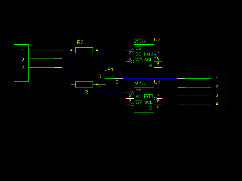
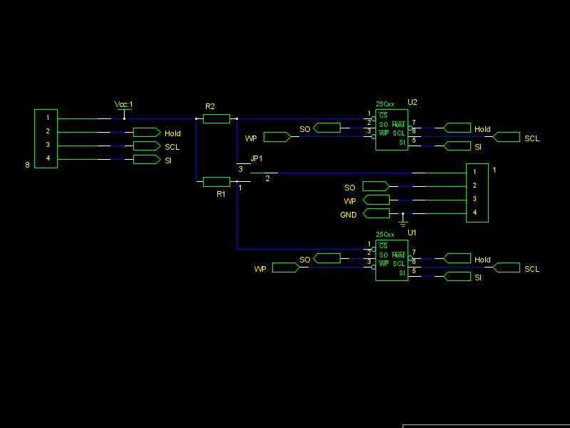
So after a weekend and some playing with gEDA and pcb (learning curve that was) I drew up a schema [1] from what we talked about earlier.
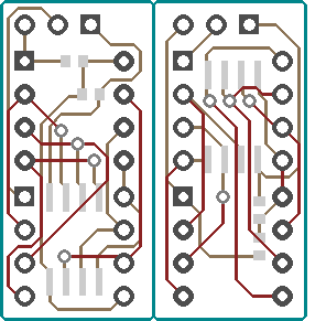
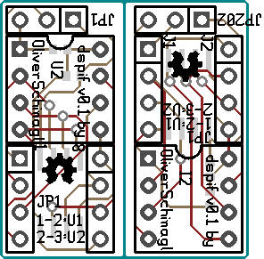
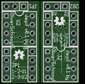
After spending some hours routing I decided to make a second version (there is plenty of room on a 5x5 pcb) with the header in the middle, instead of the edge and thus a 2 design PCB was born [2]. Before I send this off to the PCB fab and have some boards made, I was hoping what you guys thought and whether it is sound. I've attached a more or less 'complete' render [3] and one without the silkscreen [4] (probably most usefull).
(M)any pointers appreciated, this being my first board ever designed :)
[1] dspif_sch.png [2] dspif_photo.png [3] dspif.png [4] dspif_nosilk.png
On 03/07/12 16:28, Oliver Schinagl wrote:
On 06-03-12 19:33, Peter Stuge wrote:
Oliver Schinagl wrote:
Pin 1, 'chip select enable' is an inverted? pin. enables and disables device operation. When chip select is high, the device is de-selected and the serial data pins are at 'high impedance'.
Correct.
So if I understand all this correctly, the chip can be connected in parallel with the exception of the Chip Select Enable. A simple switch to either connect it directly to the board/socket/other end and toggle it to connect to ground (via 'some' resistor').
Right. This is what you can see demonstrated in the photos linked to at the bottom of http://stuge.se/m57sli/ i.e.:
http://stuge.se/m57sli/overview.jpg http://stuge.se/m57sli/U5.jpg http://stuge.se/m57sli/U9.jpg
These photos are not from a PC mainboard but the principle hopefully shows. The connection you describe is indeed how GIGABYTE boards implement Dual BIOS. What is not shown in my photos are the resistors, which are mounted onto the GIGABYTE board on pads for that very purpose.
After this mail-conversation, those images make perfect sense!
I tried to make a simple schematic in ascii, but failed horribly so i've attached it to this message as monochrome BMP (only format that I could quickly think of to be smallest in size).
Hint: png
I thought I tried and came out to 54kb, I redid them in this new version and it is only 998 bytes! Nice!
I don't know what value those resistors need to be (and if the schematic can be even more simplified, with a single resistor), but I belive this is the schematic used for the dual-SPI flash 'module'
Not quite, the resistors need to be pull-up and not pull-down. See e.g. http://stuge.se/flash_switch.png which shows the principle with resistors, but connects the switch common to GND, instead of to the mainboard as must be done.
Hmm, I made a new 'design' and I put the common of the switch to the GND, but you say it should connect to the motherboard? Why is this?
This seems sensible to me, but my knowledge in this field is very limited.
You're already learning more. Your schematic is correct, but resistors need to pull up to 3.3V and not down to GND. The values are, as I wrote earlier, not really critical, just don't go too much under 1k or you will potentially waste some current.
Also make sure that your switch is the break-before-make type.
Learn I did, I'll now try to learn some gEDA and design a basic PCB for this purpose!
//Peter
Oliver Schinagl wrote:
I've attached a more or less 'complete' render
Please just send the .pcb so that I can open it. Also, the schematic is not very clear.
//Peter
On 03/21/12 04:42, Peter Stuge wrote:
Oliver Schinagl wrote:
I've attached a more or less 'complete' render
Please just send the .pcb so that I can open it. Also, the schematic is not very clear.
//Peter
I've attached the .pcb and a more clear version of the schematic. I was just dabbling with geda's schematic editor and first wired everything together. It got very messy so decided to just put the net definitions directly on the pins. This is still the case, but with proper input/output markers hopefully.
Oliver
I just noticed I've attached the old version of the schematic. Thus a freshly generated schema.
Oliver
On 03/22/12 01:58, Oliver Schinagl wrote:
On 03/21/12 04:42, Peter Stuge wrote:
Oliver Schinagl wrote:
I've attached a more or less 'complete' render
Please just send the .pcb so that I can open it. Also, the schematic is not very clear.
//Peter
I've attached the .pcb and a more clear version of the schematic. I was just dabbling with geda's schematic editor and first wired everything together. It got very messy so decided to just put the net definitions directly on the pins. This is still the case, but with proper input/output markers hopefully.
Oliver

Hi,
the schematic looks good. Sorry I haven't noticed this thread earlier. I don't know what's your mainboard, but I had some problems with mine since EFI writes to flash during power up?/down? cycles and doesn't like hot switched chip during poweroff. Anyways, better be prepared to use external programmer, like „wiggler clone“ in case of everything fails.
Goodluck, Tadas (Mrtadis)

On 03/26/12 22:54, Tadas Slotkus wrote:
Hi,
the schematic looks good. Sorry I haven't noticed this thread earlier. I don't know what's your mainboard, but I had some problems with mine since EFI writes to flash during power up?/down? cycles and doesn't like hot switched chip during poweroff. Anyways, better be prepared to use external programmer, like „wiggler clone“ in case of everything fails.
Goodluck, Tadas (Mrtadis)
Thanks, if people here atleast all agree that its sound, I'll send it off to seeed to have it printed.
From what I understood, SPI is a shared bus, so Chip Select 0/1 should allow you to switch between various chips/eeproms.
So even if one's motherboard is completly weird, I guess having chipselect on chip 1 first, boot, then while booted swap to 2, flash new bios, switch back to 1, shutdown. This should work (I cannot image the bios/uefi, constantly writing to the eeprom?
Then when powerd down, move your jumpercap/switch back to the newly flashed eeprom and you should be golden. If the new flash is coreboot, it shouldn't be a problem anymore, if the new flash is some other bios/uefi, then take caution when swapping.
But this is what I suspect, I'm sure there's many more people on this list who actually really know what happens ;)
Oliver
Hi list,
Unfortunately I have had little feedback so far. But here's a small update.
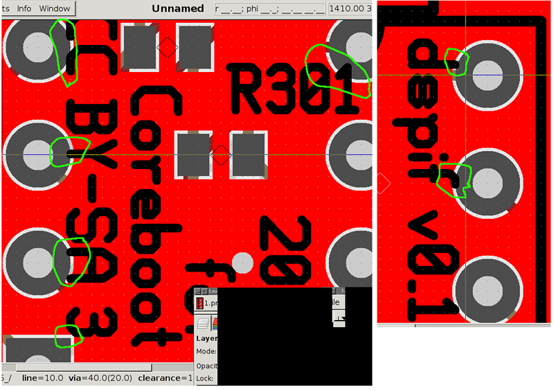
I have finally received my SO8 memory modules and those babies are small. Because of this, I have replaced the SO8M footprint with an SO8W footprint, making it quite a bit wider, but should be much easier to manually solder. I tried for an hour to fit a 1008 footprint for the resistors but there would be hardly any room left for silkscreening. Also all the smd compontens that I have to salvage seem to be 0603 components anyway. I'm sure people will manage to solder 2 resistors.
I've also saw a screenshot of an Asus motherboard that had the bios chip right next to a Sata port, in the wrong/different orientation, so I've added a 3rd design so all 3 possible insertations are possible. (Left, center and right facing connector).
I've attached the gEDA .pcb file with the 3 orientation, with each having their individually nets/defs so that the DRC/rat check works. When sending out the final rev. I'll copy/paste the silk screens from the left design so they all look identical.
If I get no negative feedback, I'll try to send the boards out for manufacture next week, so in a month or two I should have about 40 PCB's and would be happy to send a few out to coreboot dev's, if there's any interest at all :)
Oliver
Oliver Schinagl wrote:
Unfortunately I have had little feedback so far. But here's a small update.
Thanks for the update.
I did look at your previous board but needed more time to really look closely.
I have finally received my SO8 memory modules and those babies are small.
Oh it's not so bad. :) Try the 0603 resistors.
Because of this, I have replaced the SO8M footprint with an SO8W footprint,
This is actually correct. All SPI flash chips used in PCs are in the 200 mil wide package, not the standard SO8 which is only 150 mil.
I've also saw a screenshot of an Asus motherboard that had the bios chip right next to a Sata port, in the wrong/different orientation, so I've added a 3rd design so all 3 possible insertations are possible. (Left, center and right facing connector).
Ah, so the plan is that your PCB is plugged into the factory BIOS socket? That's a nice idea, but as you discovered there are four ways that the chip can be oriented, so you really have to make four boards to have a solution that works on every board. :\
I've attached the gEDA .pcb file with the 3 orientation,
Thanks. I'll try to give some more detailed feedback, but one big no-no that I've seen already is that your silk is covering pads. Noone will do any cropping for you, so you will indeed get silkscreen on your pads, which 1) potentially makes the board house unhappy because it may make a mess in their machines, and 2) makes it difficult for solder to flow over the pad.
When sending out the final rev. I'll copy/paste the silk screens from the left design so they all look identical.
No, please do not make design changes post final review. Another way to express this is please only send files for review that you believe that you are finished with. Of course there can be iterations and that's fine! But don't make further changes after the final iteration.
//Peter
On 04/05/12 01:23, Peter Stuge wrote:
Oliver Schinagl wrote:
Unfortunately I have had little feedback so far. But here's a small update.
Thanks for the update.
I did look at your previous board but needed more time to really look closely.
That would be grand!
I have finally received my SO8 memory modules and those babies are small.
Oh it's not so bad. :) Try the 0603 resistors.
Because of this, I have replaced the SO8M footprint with an SO8W footprint,
This is actually correct. All SPI flash chips used in PCs are in the 200 mil wide package, not the standard SO8 which is only 150 mil.
There are 3 SO8 package footprints in PCB, SO8, SO8M and SO8W. None fit 'perfectly'. S08 is way to small to be usefull, SO8M fits 'perfectly' but makes it extremly hard to solder I recon, since the pad, ends at the legs. SO8W seems to be a little to wide, the legs end up perfectly on the inner sides, which might make it not to cover the back 'cavities' perfectly? But I guess it will have to do.
The PCB's that I used as inspiration actually do fit perfectly :)
http://www.ebay.com/itm/10-pc-SOIC-8-DIP-8-Narrow-PCB-SMD-Adapter-DIP-/40022...
I've also saw a screenshot of an Asus motherboard that had the bios chip right next to a Sata port, in the wrong/different orientation, so I've added a 3rd design so all 3 possible insertations are possible. (Left, center and right facing connector).
Ah, so the plan is that your PCB is plugged into the factory BIOS socket? That's a nice idea, but as you discovered there are four ways that the chip can be oriented, so you really have to make four boards to have a solution that works on every board. :\
Yes, the plan was to have the PCB go into the motherboard, and the original bios piggy bags ontop! The
Well, 4 orientations, but I think 1 can be used for 2 orientations. It all depends on what is blocking your board however.
I hope it's quite unlikly that a bios is constrained on 3 sides, but as always possible. If I get bored later this week, I may end up making the missing 4th design then, where the socket sits 'sideways'. Should be considerably easier to route then the ones I have now ...
I've attached the gEDA .pcb file with the 3 orientation,
Thanks. I'll try to give some more detailed feedback, but one big no-no that I've seen already is that your silk is covering pads. Noone will do any cropping for you, so you will indeed get silkscreen on your pads, which 1) potentially makes the board house unhappy because it may make a mess in their machines, and 2) makes it difficult for solder to flow over the pad.
Hmm, I assumed silk screening is applied last, as I have seen soldermasks and silkscreening covering via's. The only thing I cover IS via's ... because of that assumption.
When sending out the final rev. I'll copy/paste the silk screens from the left design so they all look identical.
No, please do not make design changes post final review. Another way to express this is please only send files for review that you believe that you are finished with. Of course there can be iterations and that's fine! But don't make further changes after the final iteration.
I should have clarified this yes, I would of course have posted the final version that would have been sent off to the board house. But that version will fail DRC checking :(
//Peter
Oliver Schinagl wrote:
There are 3 SO8 package footprints in PCB, SO8, SO8M and SO8W. None fit 'perfectly'.
I'll see if I can send you a footprint I've used.
Thanks. I'll try to give some more detailed feedback, but one big no-no that I've seen already is that your silk is covering pads. Noone will do any cropping for you, so you will indeed get silkscreen on your pads, which 1) potentially makes the board house unhappy because it may make a mess in their machines, and 2) makes it difficult for solder to flow over the pad.
Hmm, I assumed silk screening is applied last, as I have seen soldermasks and silkscreening covering via's. The only thing I cover IS via's ...
No. See attached file, or http://stuge.se/4.png if it gets stripped from the list.
//Peter
-
 Oliver Schinagl
 -
 Oliver Schinagl
 -
 Peter Stuge
 -
 Tadas Slotkus